
-
-
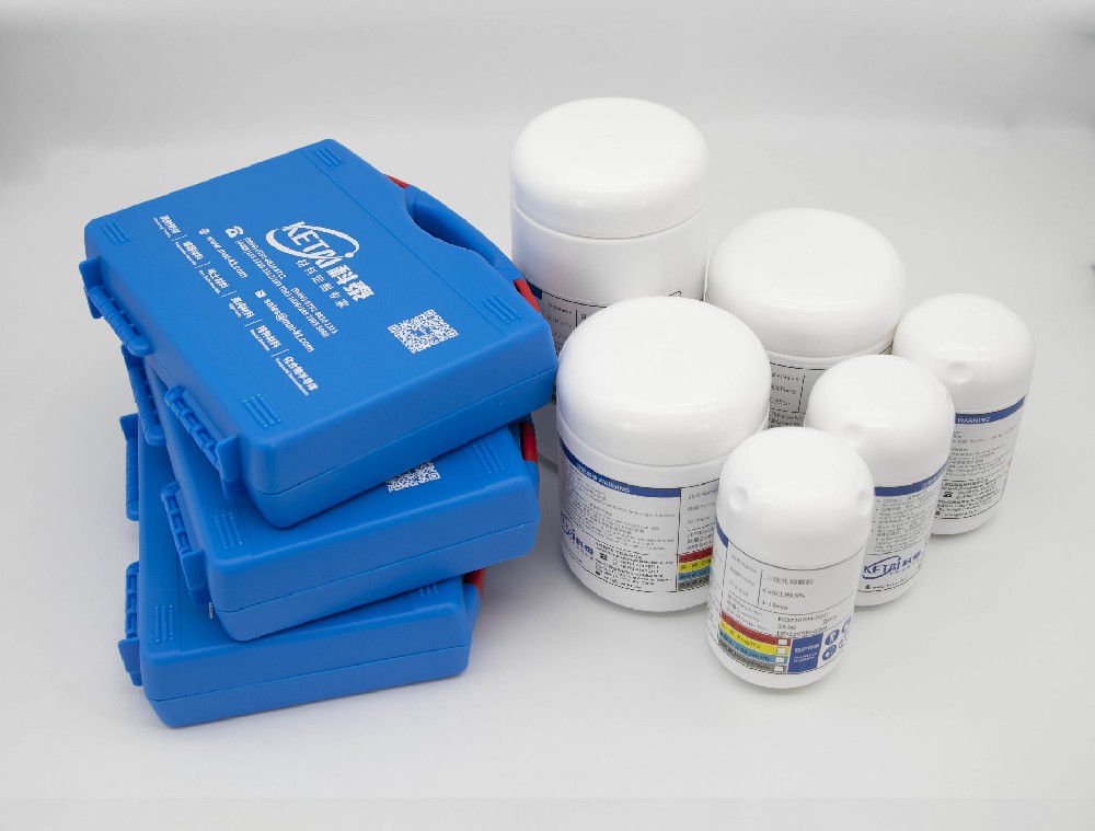
Sputtering Targets
- Element Sputtering Targets
- Alloy Sputtering Targets
- Oxide Sputtering Targets
- Nitride Sputtering Targets
- Carbide Sputtering Targets
- Fluoride Sputtering Targets
- Silicide Sputtering Targets
- Sulfide Sputtering Targets
- Selenide Sputtering Targets
- Telluride Sputtering Targets
- Antimonide Sputtering Targets
- Phosphide Sputtering Targets
- Special Sputtering Targets Customization
- Sputtering Targets List
-
Evaporation Materials
- Element Evaporation Materials
- Alloy Evaporation Materials
- Oxide Evaporation Materials
- Nitride Evaporation Materials
- Carbide Evaporation Materials
- Fluoride Evaporation Materials
- Phosphide Evaporation Materials
- Telluride Evaporation Materials
- Selenide Evaporation Materials
- Sulfide Evaporation Materials
- Other Evaporation Materials
- Evaporation Materials List
- Compound Semiconductor Materials
- Rare Earth Materials
- Special Alloy
-
Crucible customization
-
Sputtering Targets


- H氢Hydrogen
- He氦Helium
- Li锂Lithum
- Be铍Beryllium
- B硼Boron
- C碳Carbon
- N氮Nitrogen
- O氧Oxygen
- F氟Fluorine
- Ne氖Neon
- Na钠Sodium
- Mg镁Magnesium
- Al铝Aluminium
- Si硅Silicon
- P磷Phosphorus
- S硫Sulfur
- Cl氯Chlorine
- Ar氩Argon
- K钾Potassium
- Ca钙Calcium
- Sc钪Scandium
- Ti钛Titanium
- V钒Vanadium
- Cr铬Chromium
- Mn锰Manganum
- Fe铁Iron
- Co钴Cobalt
- Ni镍Nickel 2
- Cu铜Copper
- Zn锌Zinc
- Ga镓Gallium
- Ge锗Germanium
- As砷Arsenic
- Se硒Selenium
- Br溴Bormine
- Kr氪Krypton
- Rb铷Rubidium
- Sr锶Strontium
- Y钇Yttrium
- Zr锆Zirconium
- Nb铌Niobium
- Mo钼Molybdanium
- Tc碍Technetium
- Ru钌Ruthenium
- Rh铑Rhodium
- Pd钯Palladium
- Ag银Silver
- Cd镉Cadmium
- In铟Inlium
- Sn锡Tin
- Sb锑Antimony
- Te碲Tellurium
- I碘Iodine
- Xe氙Xenon
- Cs铯Caesium
- Ba钡Barium
- LaLu镧系LaLu
- Hf铪Hafnium
- Ta钽Tantalum
- W钨Tungsten
- Re铼Rhenium
- Os锇Osmium
- Ir铱Iridium
- Pt铂Platinum
- Au金Gold
- Hg汞Mercury
- Tl铊Thallium
- Pb铅Lead
- Bi铋Bismuth
- Po钋Polonium
- At砹Astatium
- Rn氡Radon
- La镧Lanthanum
- Ce铈Cerium
- Pr镨Praseodymium
- Nd钕Neodymium
- Pm钷Promethium
- Sm钐Samarium
- Eu铕Europinu
- Gd钆Gadolinium
- Tb铽Terbium
- Dy镝Dysprosium
- Ho钬Holmium
- Er铒Erbium
- Tm铥Thulium
- Yb镱Ytterbium
- Lu镥Lrtetium
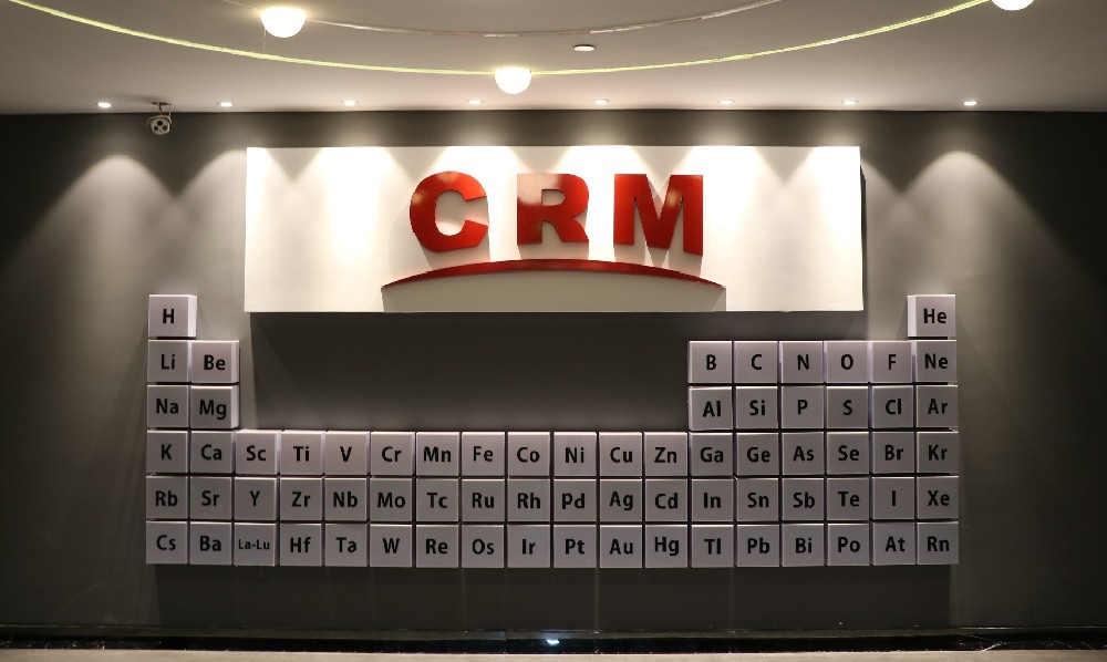
Click to view the relevant product information containing the corresponding elements
Ketai new materials can provide customization of any combination of materials with almost all elements (except radioactive elements) in the "yuansuo periodic table". Some products have not been updated in time. Please consult customer service for special customization needs.
- H氢Hydrogen
- He氦Helium
- Li锂Lithum
- Be铍Beryllium
- B硼Boron
- C碳Carbon
- N氮Nitrogen
- O氧Oxygen
- F氟Fluorine
- Ne氖Neon
- Na钠Sodium
- Mg镁Magnesium
- Al铝Aluminium
- Si硅Silicon
- P磷Phosphorus
- S硫Sulfur
- Cl氯Chlorine
- Ar氩Argon
- K钾Potassium
- Ca钙Calcium
- Sc钪Scandium
- Ti钛Titanium
- V钒Vanadium
- Cr铬Chromium
- Mn锰Manganum
- Fe铁Iron
- Co钴Cobalt
- Ni镍Nickel 2
- Cu铜Copper
- Zn锌Zinc
- Ga镓Gallium
- Ge锗Germanium
- As砷Arsenic
- Se硒Selenium
- Br溴Bormine
- Kr氪Krypton
- Rb铷Rubidium
- Sr锶Strontium
- Y钇Yttrium
- Zr锆Zirconium
- Nb铌Niobium
- Mo钼Molybdanium
- Tc碍Technetium
- Ru钌Ruthenium
- Rh铑Rhodium
- Pd钯Palladium
- Ag银Silver
- Cd镉Cadmium
- In铟Inlium
- Sn锡Tin
- Sb锑Antimony
- Te碲Tellurium
- I碘Iodine
- Xe氙Xenon
- Cs铯Caesium
- Ba钡Barium
- LaLu镧系LaLu
- Hf铪Hafnium
- Ta钽Tantalum
- W钨Tungsten
- Re铼Rhenium
- Os锇Osmium
- Ir铱Iridium
- Pt铂Platinum
- Au金Gold
- Hg汞Mercury
- Tl铊Thallium
- Pb铅Lead
- Bi铋Bismuth
- Po钋Polonium
- At砹Astatium
- Rn氡Radon
- La镧Lanthanum
- Ce铈Cerium
- Pr镨Praseodymium
- Nd钕Neodymium
- Pm钷Promethium
- Sm钐Samarium
- Eu铕Europinu
- Gd钆Gadolinium
- Tb铽Terbium
- Dy镝Dysprosium
- Ho钬Holmium
- Er铒Erbium
- Tm铥Thulium
- Yb镱Ytterbium
- Lu镥Lrtetium
ABOUT KETAI
current location:Home >> About >> Company Profile
COMPANY PROFILE
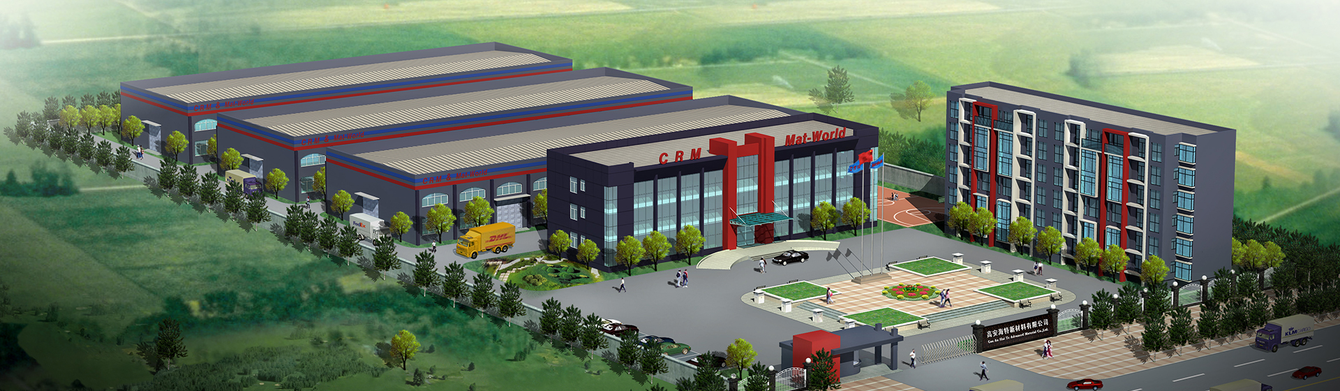
Jiangxi Ketai Advanced Materials Co., Ltd. is a national high-tech enterprise that provides "one-stop material customization" production for global material workers.
Ketai technical team took the lead in providing "material customization services" for overseas customers in 2004. In 2009, Jiangxi Ketai Advanced Materials Co., Ltd. was established to carry out material customization production, with an investment of 75million to build a 25 mu material customization factory in Jiangxi Gao'an development zone.
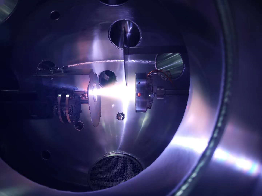
After 18 years of hard work, Ketai has grown into an internationally recognized "laboratory factory" of functional materials. Ketai has comprehensive and diverse production and testing equipment and production technology in various fields, and has accumulated production experience of almost all elements (except radioactive elements) in the "periodic table of elements".
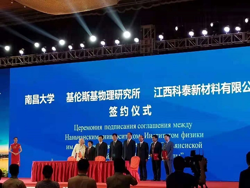
Ketai takes "Yichun functional film material research center", "Jiangxi functional material and film research center" and "Russian kirensky Institute of physics" as the core technical team. The technical team is composed of experienced experts in the material industry at home and abroad, specializing in semiconductor material synthesis, vacuum hot pressing, vacuum melting, rare earth materials, machining, analysis and testing, etc.
Ketai adopts the professional technical team and process combination of "four in one" (powder metallurgy, vacuum smelting, compound semiconductor, rare earth smelting), and has created many advanced high-tech products for international customers. The products are widely used in aerospace, scientific research, moled, 5g, semiconductor chips, storage, optics, solar cells, displays, touch screens, electronic devices, tool modification and other fields.
After years of technological precipitation, Ketai has a number of products with independent intellectual property rights that can be scaled up and industrialized. In 2019, Ketai invested 200million yuan to build a 30 mu Industrial Park in Jiangxi Nanchang Airport Development Zone. Relying on the comprehensive material customization technology advantages of Ketai Gao'an factory, the industrial park will deeply understand the "material pain points" of the industry, provide customers with long-term "technical companionship" through practical and accurate material solutions and professional technical support services, and enable enterprise customers to innovate products and develop large-scale applications of new materials. The industrial park is planned to be officially put into operation in 2022, and its output value is expected to reach 200million yuan in 2022.
In the future, Ketai will uphold the corporate vision of "becoming an expert in material solutions" and create a better future with global material workers with more professional technology, better product quality and better technical services!

-

18
Established for 18 years
-

2
2 large production base
-

1500
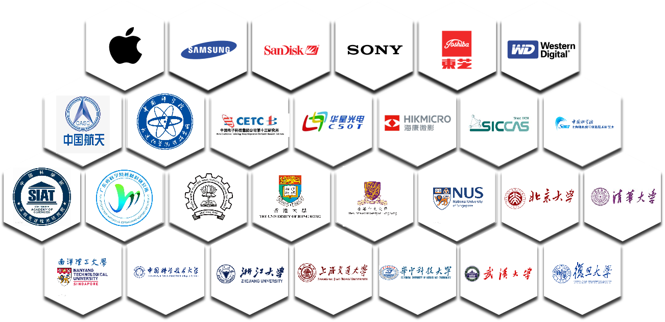
More than 1500 well-known cooperative enterprises
APPLICATION AREA
-
APPLICATION
Ketai adopts the professional technical team and process combination of "four in one" (powder metallurgy, vacuum smelting, compound semiconductor, rare earth smelting), and has created many advanced high-tech products for international customers. The products are widely used in aerospace, scientific research, moled, 5g, semiconductor chips, storage, optics, solar cells, displays, touch screens, electronic devices, tool modification and other fields.
-
TEAM
Ketai takes "Yichun functional film material research center", "Jiangxi functional material and film research center" and "Russian kirensky Institute of physics" as the core technical team. The technical team is composed of experienced experts in the material industry at home and abroad, specializing in semiconductor material synthesis, vacuum hot pressing, vacuum melting, rare earth materials, machining, analysis and testing, etc.


DEVELOPMENT HISTORY
CUSTOMER PRESENTANTION

-

Wechat scan real-time quotation
-

YouTube Channel
-

Linkedin